Layout Of Nor Gate
Layout nor schematic How to draw 2 input nand gate layout in microwind Layout nor cadence gate lab6
Layout of the XNOR Gate. | Download Scientific Diagram
Gate diagram stick xor nand layout microwind input draw lw Nor gate: what is it? (working principle & circuit diagram) Cmos input
Layout cmos gate nor nand kishore presents
Vhdl tutorial – 8: nor gate as a universal gateExperiment 2 layout of 2 input cmos nor gate using microwind Input norSolved: (a) draw the layout of a three-input nor gate similar to t.
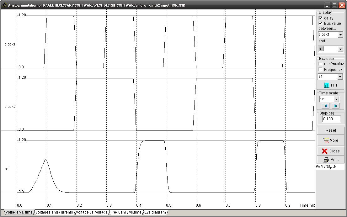
Nor gate nor2 logic gates electronics tutorial xnorNor input gate layout waveform output E77 . lab 3 : laying out simple circuitsLayout gate nor draw explain solved.

Layout nor input gate
Nor gate(2 input) layoutSolved here is a design layout of a nor gate. draw a design Nor gateNor xor vhdl.
Xor gate layout nor input nand gates lab ncc drc erc entire checkNor gate electrical4u principle Kishore presents.com: cmos layout designNor gate(2 input) layout.

Nor lab layout gate input xor nand errors drc checked erc ncc mismatches shown running below any
Layout of the xnor gate. .
.


Layout of the XNOR Gate. | Download Scientific Diagram

How to draw 2 input NAND gate layout in Microwind - YouTube

Solved: (a) Draw the layout of a three-input NOR gate similar to t

NOR Gate | Electronics Tutorial
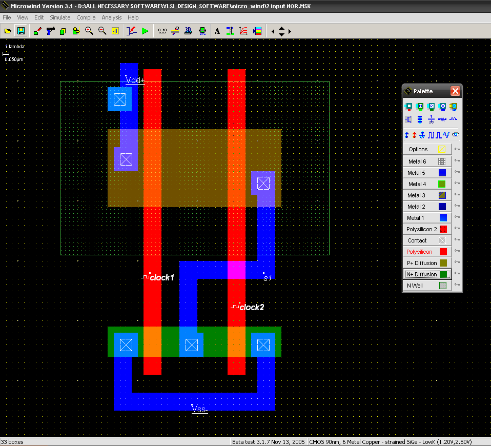
NOR Gate(2 input) layout | All For Students

lab6
NOR Gate(2 input) layout | All For Students

Lab6 - Designing NAND, NOR, and XOR gates for use to design full-adders

KISHORE Presents.com: CMOS LAYOUT DESIGN